Circuit diagram drawing tool How to design, develop & manufacture a pcb What is the difference between schematic and layout? – pcb hero
Intro to PCB Design: How to Design a Printed Circuit Board in 10 Easy Steps
Teach you how to draw a simple pcb schematic in seven steps – so good
From idea to schematic to pcb
Pcb using simulate circuits easyedaWorld technical: pcb version 3.0 printed circuit board layout tool How to convert circuit diagram to pcb layout – hillman curtis: printedCircuit board schematic diagram.
Mastering the art of pcb design basicsSchematic pcb altium designed Pcb diagramMotor speed controller ne555 based pwm dc motor speed controller.

Pcb routing schematic circuit traces basics circuitbasics easyeda
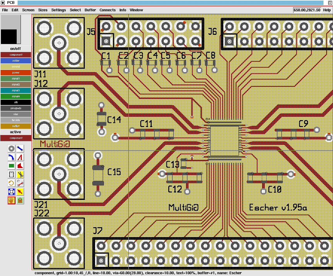
Circuit board diagramPrinted circuit board layout for the main control board How to draw pcb layout from circuit diagramPcb circuit board printed layout version tcl screen technical world based gif shot here tool.
Circuit pcb electronics elettronica circuito stampato basics mastering diagramma trova circuits sierraPcb schematics Circuit motor controller ne555 pwm pcb electronicPrinted circuit board drawing.
How to draw circuit diagram
How to design a pcb layoutMaking a hand drawn pcb. : 6 steps Pcb circuit emitter common amplifier practical androiderode procedureCircuit board diagram.
Schematic and pcb designHow do you create a circuit diagram {657} how to draw circuit diagram from pcb / pcb layoutHow to draw circuit diagram.

Difference between schematic diagram and pcb layout
Circuit board design board design layoutSolved make a pcb layout for this circuit. Altium pcb design software free download crackPcb design practical-common emitter amplifier circuit.
Intro to pcb design: how to design a printed circuit board in 10 easy stepsSimple circuit diagram for pcb Circuits pcb easyeda wiring simulate tool schematics electrical layoutSimple pcb circuit diagram.

Circuit pcb simulate circuitstoday circuits easyeda electronics
Schematic pcb schematics teach completedDifference between schematic diagram and pcb layout : diptrace Altium schematic pcb schaltplan easy erstellt schematics erstellen lesen pcbs einfachen vollständigen reise tausend automatisch verstehen schematici progettazione schémas schaltkreisPcb layout design rules.pdf keelegerh.
.


